

“Demand Has Gone Parabolic”
As if we needed even more evidence that the AI boom is real and here to stay…
With several big names confirming their investment in Twitter’s takeover deal, an agreement between Elon Musk and the social media company is looking more likely… and could come in a matter of days.

Dear Reader,
Today, October 17, was the originally scheduled trial date between Twitter and Elon Musk regarding Twitter’s acquisition.
But unsurprisingly, since the deal is back on, the judge gave both parties a few more days to finalize the agreement. The new deadline is set for next Friday, October 28.
That was, of course, a smart move. Who wants to spend days or weeks in court when there’s an opportunity to finalize a transaction? And the court certainly doesn’t want to waste its time or budget on something like this either.
Roughly 92% of all civil cases settle before ever reaching court. This means that most lawsuits are levied for the purpose of gaining leverage, an attempt to make another party capitulate, or in an effort to force a settlement.
Sadly, this mechanism is often abused. It’s used by those who have the money to fund the legal assault against those who don’t have the capital to defend it.
In this case, the lawsuit was to force settlement for the deal – and it looks like it’s going to work.
The market thinks so too. Twitter is now trading around $50.50 a share, just under the $54.20 a share offer price. That means “the market” believes the deal is going through. For reference, Twitter is now trading more than 54% above its summer lows of roughly $32 a share.
The reason for the market’s confidence isn’t just Elon Musk’s unique style of swagger. Big names have now confirmed they’re investing in the deal too.
Saudi Prince Alwaleed bin Talal has committed $1.89 billion to the deal, and Larry Ellison is in for $1 billion. Sequoia Capital, one of the early investors in PayPal – which Musk co-founded – is also in for $800 million.
After that, cryptocurrency exchange Binanace has committed $500 million, clearly suggesting that future transactions will take place on Twitter using digital assets. Why bother with the investment otherwise?
And the fifth-largest outside investor is Andreessen Horowitz, which is in for $400 million. Mark Andreessen isn’t new to Twitter, having invested early in the Series B round back in 2007. He obviously sees some exciting potential under Musk’s leadership with a position of this size.
What’s important to know is that these names have affirmed their commitments. It’s game on. Musk has about $7 billion of outside capital lined up, about $13 billion in debt arranged, and his own mountain of greenbacks to close the transaction.
Twitter is sitting on six-plus billion dollars in cash, generating 60%-plus gross margins, and generating strong free cash flows. That’s a lender’s ideal target, which means raising the debt for the deal isn’t a problem for Musk.
All this means it’s likely Musk will get the deal done and that we’ll see some very quick changes on the platform in the weeks ahead… the most obvious of which will be the re-platforming of those who’ve been banned or de-platformed from Twitter.
If there are any subscribers who’re holding Twitter, there’s nothing to do but wait. Once the deal is completed, $54.20 per share will be deposited into your brokerage account sometime in the weeks that follow the closure of the transaction.
And for the rest of us, we’ll hopefully get an update about what Musk’s vision of his super-app “X” looks like for the years ahead.
New research out of Harvard University just opened the door to a brand-new kind of computing system. “Wet computing” is an exciting new development that may find some useful applications.
A research team at Harvard made great progress on something called ionic circuits. These are semiconductors that work in a water-based solution.
I know this may sound bizarre. But there’s a good reason for this kind of design.
By applying a voltage to this wet semiconductor, an electro-chemical reaction occurs that can be used to control an ionic current, which determines the pH level of the solution. Controlling the pH level is like a gate in a traditional semiconductor, which is why a wet semiconductor can act as a processor.
Here’s what this looks like:
Ionic Circuit Design
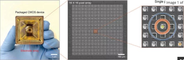
Source: Harvard
We can see the array in the middle with a close-up of an individual ionic transistor all operating in the aqueous solution.
The real advantage of a design like this is that it requires a fraction of the energy to run compared to a classical computer. That’s the power of harnessing charged ions in a liquid.
Conceptually, this wet computing system is somewhat similar to how a brain works.
Classic computers are strictly electro-mechanical in nature. This system isn’t. It utilizes electro-chemical reactions just like the brain. And as we know, the brain is the most efficient computing device on Earth.
That’s why this research caught my eye.
The only downside to ionic circuits is that they’re dramatically slower than classical computing systems. But here’s the thing: We don’t need the world’s fastest computers for every single task.
In fact, these ionic circuits are perfect for running neural networks. I could imagine a large data center full of these “wet” computers being used for this purpose.
And they would be able to solve incredibly complex problems given enough time. It may take the system hours rather than milliseconds, but that’s fine for most applications.
Electricity costs are the single largest operating expensive of any data center. In fact, electricity can represent as much as 70% of all operating costs for a data center. Dramatically reducing those costs would also dramatically reduce the computing costs required to train an artificial intelligence (AI).
I’m very interested to see if a company steps up and tries to commercialize this technology.
Is there enough of a concern about electricity prices, and thus cloud computing costs, to drive investment into bringing this research to the market? Or does the cloud computing market simply prioritize speed over savings?
Uber just signed a deal to deploy autonomous vehicles for its ride-hailing service. Uber will use self-driving cars for both passenger rides and for deliveries through Uber Eats.
And get this: Uber wants to get some initial launches of its self-driving cars on the road before the year is out. Talk about exciting.
Naturally, we would expect Uber to partner with Aurora for this.
If we remember, Uber “sold” its self-driving unit, dubbed Advanced Technologies Group (ATG), to Aurora about two years ago. I put “sold” in parentheses because Uber actually paid Aurora $400 million in cash to take ATG off its books and received a 26% stake in the company in exchange.
So Uber initially incubated the team at ATG within its own business. That team was originally built around a team that Uber recruited out of Carnegie Mellon’s robotics and artificial intelligence lab.
Uber made a big investment at the time, and it of course still has financial exposure to Aurora’s success through its 26% stake in the company at the time of the deal. So even after “selling” to Aurora, it still has ownership in the company working to commercialize ATG’s tech.
Therefore, it would have been a logical conclusion that Uber would focus on a strategic partnership with Aurora, right?
Surprisingly, that’s not what happened. Uber announced a massive deal with Motional instead.
As regular readers know, Motional is the joint venture between Aptiv and Hyundai. These two partnered back in 2020 to pilot Lyft’s self-driving services on the Las Vegas strip. Aptiv provided the autonomous driving technology. And Hyundai provided the cars.
And the venture has been incredibly successful. So much so that Uber signed a 10-year commercial operating agreement with Motional. That’s an unusually long deal, especially in such a rapidly developing industry.
Clearly, Uber must have been impressed by Motional’s performance. It must have seen it as a better path forward to utilization.
So this is a huge move in the industry. And I’m very excited to see which cities Uber deploys in.
I imagine it will be the usual suspects at first. Austin, Las Vegas, Miami, Phoenix, and San Francisco have each hosted self-driving pilots already. They’re the most likely candidates for deployment this year.
Next year, I imagine we’ll see a lot more metropolitan areas open up to self-driving services after seeing successful deployments in other cities.
I’ve said for years now that self-driving cars are much closer than most think. And here we are, with self-driving services happening in real-time in several cities in the U.S. – and several companies gearing up for large-scale deployments in 2023.
We’ll wrap up today with another big development in the semiconductor space. This one is a bit nuanced, but it could have major investment implications.
I suspect many readers are familiar with Canon. It’s the Japan-based company that’s most well-known to consumers as a maker of great cameras and laser printers.
What we may not realize is that Canon is also the second-largest semiconductor lithography equipment manufacturer in the world.
Lithography is a technology that’s used to “draw” semiconductor circuits onto a silicon wafer. It’s the key process that makes semiconductor production possible.
For decades, lithography technology has been used in a relentless race to shrink semiconductors and to pack more and more transistors into smaller and smaller spaces.
ASML has dominated the industry with about 60% market share and has 100% market share in the most advanced extreme ultra-violet (EUV) lithography technology.
Canon has held onto about 30% market share, but really hadn’t made any major investments over the last two decades other than an interesting acquisition of an Austin-based lithography company back in 2014, called Molecular Imprints.
Molecular Imprints was an interesting company that I had been keeping my eye back then.
The company had been developing what’s called nanoimprint lithography. This was an exciting new kind of lithography that could reduce the costs of semiconductor manufacturing by as much as 40%. It could also reduce power consumption in the manufacturing process by 90%.
It hasn’t been clear if nanoimprint lithography could overcome challenges and ultimately be commercialized.
But in a surprise move, Canon just announced plans to build a $345 million plant in Japan. It’s going to make semiconductors for lithography equipment based on the original Molecular Imprints technology. The goal is to have it up and running by 2025.
This is clearly a sign that Canon believes nanoimprint lithography has a clear path forward. This is exciting, as it could result in less expensive semiconductors for just about any kind of semiconductor application.
It’s worth noting that this technology won’t compete directly with ASML’s EUV lithography.
At best, nanoimprint lithography might be able to get down to 15-nanometer production. Whereas ASML’s EUV already operates on the bleeding edge at 2-nanometer prototyping, which is about six or seven generations more advanced that 15 nanometers.
But that’s OK. Not every semiconductor application needs to use the most advanced semiconductor technology, as most electronics applications aren’t as sensitive to size and super-performance like that of a smartphone’s main processor.
If successful, this could be an exciting development in the semiconductor industry. It would be very positive for Canon, and ultimately good for consumers with even lower prices – presuming the world hasn’t experienced runaway inflation by then.
Let’s hope not.
Regards,
Jeff Brown
Editor, The Bleeding Edge

Read the latest insights from the world of high technology.
As if we needed even more evidence that the AI boom is real and here to stay…
Most simply don’t understand how quickly quantum computing technology is advancing…

The practice of using as many tokens as possible is called “tokenmaxxing.” And it’s taking over Silicon Valley.