
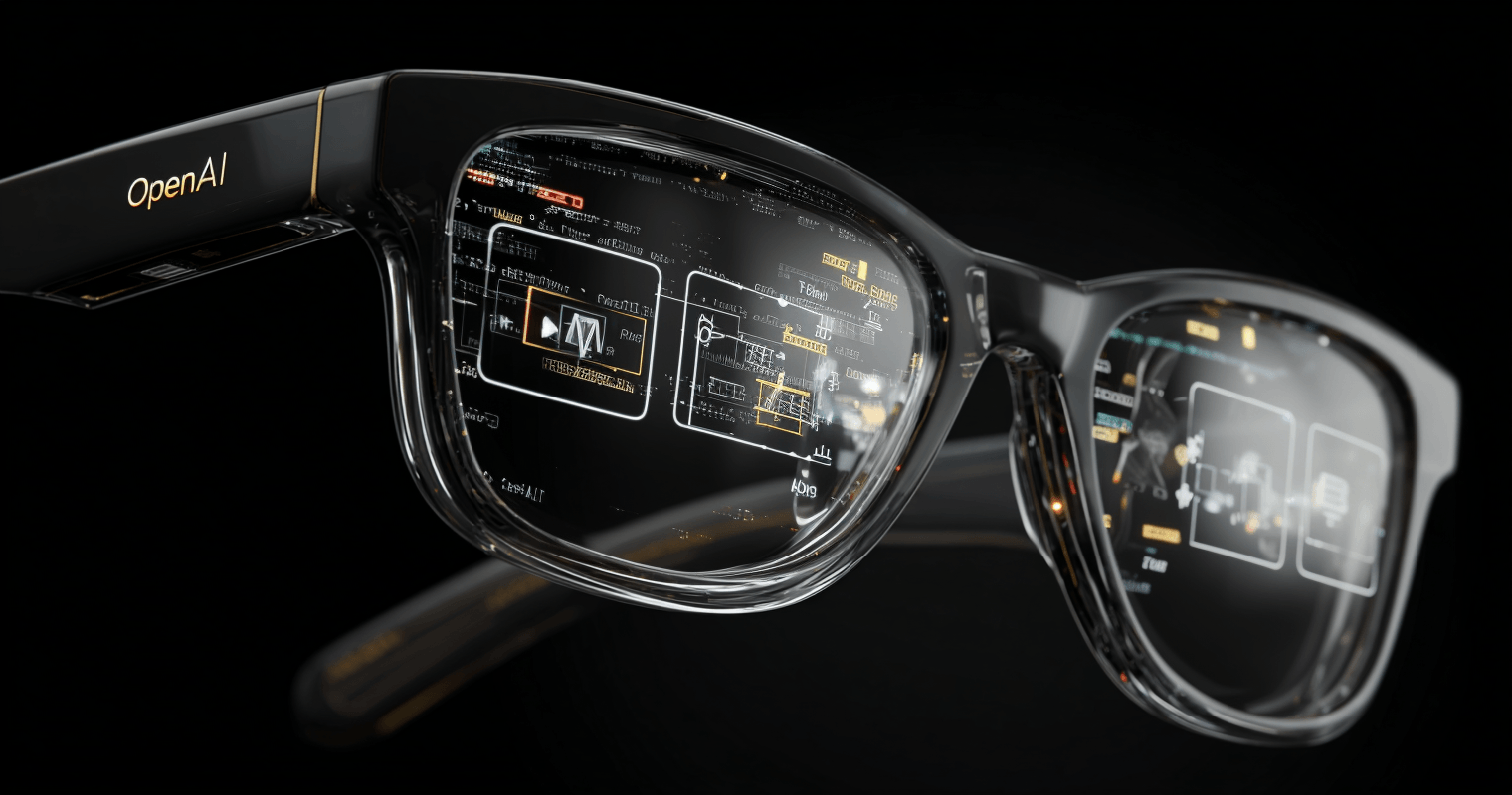
OpenAI’s Agentic AI Smartphone
We’re seeing AI-first companies working towards supplanting Google’s and Apple’s smartphone operating systems…And one of the most visible pushes...
I was saddened to learn about the recent passing of investing legend David Swensen. Today, I’d like to tell you about the amazing legacy he left behind…

Apple’s timing is no coincidence……
Lost packages will be a thing of the past…
IBM revealed some surprising news…
Dear Reader,
If there was one person that I had hoped to meet during my post-graduate studies at Yale, it was David Swensen.
During his 35-year tenure at the helm of Yale’s endowment fund, he changed the face of institutional investing. He became one of the greatest investors of all time. We can see his impact in one simple chart.

Since taking over in his early ‘30s, Swensen was responsible for growing the fund from a mere $1.3 billion to more than $31 billion today. The fund generated returns of 13.1% through June of last year and an incredible $45.6 billion in gains.
Over such a long time frame, that makes Swensen one of the best ever. And the only reason that the endowment isn’t larger is because Yale spends a portion of the endowment every year to fund operations and special projects.
What was Swensen’s secret?
Two things actually…
He was willing to play the long game. He invested in assets that had much longer times to maturity but had spectacular return profiles.
And he built a portfolio allocation model that was heavily weighted in alternative assets like hedge funds, venture capital (VC) funds, real estate, natural resources, and private equity.
Back in the ‘80s, this kind of thinking was almost nonexistent. Large institutional funds were almost entirely composed of U.S. equities, some foreign equities, cash, and fixed income.
What he started to do in the ‘90s with his asset allocation model, which he heavily weighted in alternative assets, was considered radical.
And it worked… brilliantly.
One of my favorite books of all time on investing is Swensen’s Pioneering Portfolio Management. And while it was written through the lens of managing a large, multibillion-dollar institutional portfolio over a long time horizon, many of the insights are still relevant for individual investors like us. I highly recommend reading his book.
Ultimately, as we increase our wealth over time and play our own long game, we gain access to many of the kinds of investments that Swensen was so well known for. And ultimately, our goal at Brownstone Research is to help subscribers do exactly that.
And while I’m not managing institutional money, or an endowment for that matter, my own aspirations are very similar. I intend to make my subscribers a billion dollars in profit over time with my research.
Unfortunately, I didn’t have a chance to meet with Swensen when I was at Yale. He had been battling cancer for years. I’m certain I would have liked him, though.
I was sad to hear that he passed a few days ago. We lost one of the greats, but his legacy and the impact that he had in the industry will not be forgotten.
Apple just made a big $410 million investment in optics and laser company II-VI (pronounced “two six”). This is a very telling move.
We don’t often read about Apple investing directly in companies. But the tech giant does have a not so well known program for doing so. It is called Apple’s Advanced Manufacturing Fund.
Through this program, Apple invests in companies providing key components that go into its products. It’s a way for Apple to reduce risk and support strategic suppliers in its own supply chain.
As for II-VI, it is a great company known for its vertical-cavity surface-emitting lasers (VCSELs) – pronounced “vixels.” Exponential Tech Investor subscribers know this technology well. We’re currently up 51% on II-VI in our model portfolio.
VCSELs are a key component in iPhones, starting with the iPhone 10 model. They power 3D-sensing, depth perception, and other optics-related features such as the iPhone’s Face ID. That’s the optional security feature where iPhone users can unlock their phone just by scanning their face. No pin numbers required.
So Apple clearly sees II-VI’s VCSEL technology as critical to its own business. And II-VI has been aggressively developing this technology for years now.
Back in 2019, II-VI smartly acquired a company called Finisar. Finisar had recently received a major investment from Apple’s Advanced Manufacturing Fund for its own VCSEL technology.
And earlier this year, II-VI won a bidding war for another laser company called Coherent. Bringing Coherent into the fold will strengthen II-VI’s technology offerings even more.
No doubt these aggressive moves are what spurred Apple to invest heavily in the company.
And this is about more than just features like Face ID.
II-VI’s VCSELs and light detection and ranging (LIDAR) technology are also critical to augmented reality (AR) functions. Apple’s big investment here is a major sign that AR will be a fundamental feature in each and every iPhone going forward.
And the timing isn’t a coincidence.
I am on record predicting that Apple will release the developer’s version of its first AR device this year. That will most likely happen at Apple’s developer conference in the summer.
Of course, that device will be powered by VCSELs and LIDAR as well. And that’s why Apple is making such a big investment into II-VI. It is securing the supply chain to support not only future iPhones and iPads, but also its upcoming AR device.
So this is a sign of things to come. I’ve said before that augmented reality will be the next mass-market consumer frenzy when the technology is available in a sleek form factor and attractive price point similar to the Apple Watch.
Apple’s investment in II-VI tells us that day is getting closer.
In the meantime, if readers want to learn how to invest in the companies critical to the success of the Apple iPhone… you can go right here for the full story.
Here’s a development we probably wouldn’t expect. The U.S. Post Office (USPS) is teaming up with NVIDIA and its artificial intelligence (AI) team to improve the U.S. mail system. Great news as it really needs it.
The USPS plans to use NVIDIA’s AI hardware and deep learning software to help locate lost packages more quickly. It is deploying this AI at more than 190 mail processing centers across the country.
This is a great example of AI at the edge of networks, as opposed to AI being run from a massive, centralized data center. And this edge-based AI system promises to improve efficiency tremendously.
It starts by scanning the packages and running this data through deep learning software. This enables the USPS to process package data as much as 10 times faster and more accurately than the methods previously used.
And this process generates more than 20 terabytes (TB) worth of image data every single day. For perspective, it would take 29,960 CD-ROM discs to store 20 TB worth of data. All this data helps the AI become exponentially smarter.
And the results are well worth it.
According to the USPS, it takes eight to 10 people several days to track down missing packages using its current manual process. With NVIDIA’s AI, it can locate lost packages in just a couple of hours with only one or two people involved.
So this should result in a dramatic improvement in the service we receive from the post office. Except we may not realize it. After all, we’ll simply be receiving our packages on time.
Still, this makes perfect sense. This AI technology has existed for several years now, and NVIDIA has gotten it to the point where it’s no longer too expensive to deploy.
This is just one more reason why NVIDIA is positioned to be a dominant player in the AI space for years to come.
IBM is a company that I usually don’t associate with bleeding-edge technology. However, it just claimed that it had a major breakthrough in semiconductor manufacturing. The company says that it made the first 2 nanometer (nm) chip. This is big news.
When it comes to semiconductor manufacturing, it’s all about fitting more and more transistors into a smaller space. And we do that by making the transistors smaller and putting them closer together. That’s what the nanometer number refers to. In this case, IBM says it managed to get the transistors just 2 nm apart.
This is somewhat surprising.
To start with, many smartphones and laptops in use today employ 7 nm technology. However, the newest iPhones use 5 nm chips. That’s the leading edge of semiconductor manufacturing technology available in mass production right now.
And the most advanced company in this space today, Taiwan Semiconductor Manufacturing Company (TSMC), is working on 3 nm technology behind closed doors. The fact that IBM has demonstrated 2 nm technology ahead of TSMC is quite impressive.
IBM managed to squeeze 50 billion transistors onto its 2 nm chip, which is the size of a fingernail. This can deliver about a 45% performance increase over 7 nm chips.
Alternatively, the 2 nm chip could deliver the same performance as a 7 nm chip while using 75% less energy. That would give devices a longer battery life.
For example, a 75% reduction in energy use would enable us to charge our smartphones roughly once every four days instead of every day. That’s an exciting idea for anyone who must charge their current phone twice a day.
That said, most semiconductor manufacturing companies take a blended approach.
With each improvement in semiconductor manufacturing, they take a portion of the performance increase and a portion of the energy efficiency improvement. It is always a trade-off that improves both performance and power consumption with every new generation of mobile devices.
So this is a meaningful development by IBM.
I remember a time not long ago when people said we couldn’t go smaller than 10 nm and that Moore’s Law was dead. (For newer readers, Moore’s Law says that the number of transistors in semiconductor-integrated circuits doubles every 18–24 months.) IBM is proving them wrong on all counts here.
That said, IBM won’t be able to bring this technology to market itself.
For one, IBM sold its own semiconductor foundry to GlobalFoundries back in 2014. It is no longer in the chip manufacturing business. Plus, the company has a poor record of commercializing its own breakthroughs in the lab, regardless of the tech.
However, IBM has always had a strong and fundamental approach to research and development.
So I’m excited to see this announcement. This doesn’t mean that we would want to recommend investing in IBM. We need to remember that this technology is just in IBM’s laboratory.
But if IBM can do it, I know the world’s best semiconductor foundries are going to be the first to commercialize 2 nm, or even 1 nm, as early as 2023.
We are in for some incredible times ahead.
Regards,
Jeff Brown
Editor, The Bleeding Edge
Like what you’re reading? Send your thoughts to feedback@brownstoneresearch.com.

Read the latest insights from the world of high technology.
We’re seeing AI-first companies working towards supplanting Google’s and Apple’s smartphone operating systems…And one of the most visible pushes...

About a decade’s worth of progress is happening in about 12 months regarding fourth-generation nuclear fission technology…

Early today, Tesla announced that mass production of its fully autonomous Cybercab has begun…