


The Other D.C. Cage Match
There is another type of cage match playing out in Washington right now… The bare-knuckle fight between CFTC Chairman...
Sam Altman has been scouring the globe for companies capable of building out the cutting-edge chips that power AI… And that’s because of the sheer demand that AI will have for these advanced chips. As an investor, you should be paying attention, too.
If you have $10 billion lying around, Sam Altman would like a word.
Altman is the CEO of OpenAI, the creator of the largest artificial intelligence (“AI”) platform, ChatGPT.
Last November, OpenAI’s board gave him the boot for not focusing on AI. Instead, he was jet-setting in hopes of finding investors to help him build semiconductor plants.
That’s not a small undertaking. Cutting-edge chipmaking plants cost billions of dollars and take years to build out. That’s why Altman was speaking with the likes of SoftBank and Abu Dhabi-based G42.
But Altman was brought back on as CEO of OpenAI. And last week, Bloomberg reported that he’s back on the hunt for billions in funding.
Altman and I both see the sheer demand that AI will have for advanced chips. As an investor, you should be paying attention, too.
Advanced chips are almost impossibly complex. We can count the number of companies that can build these chips with just one hand.
And AI has given the companies that make these chips a near license to print money. Elon Musk even said that he’ll buy as many as can be delivered.
Today, I’m going to share why Altman is on the right path… and how we can profit from it.
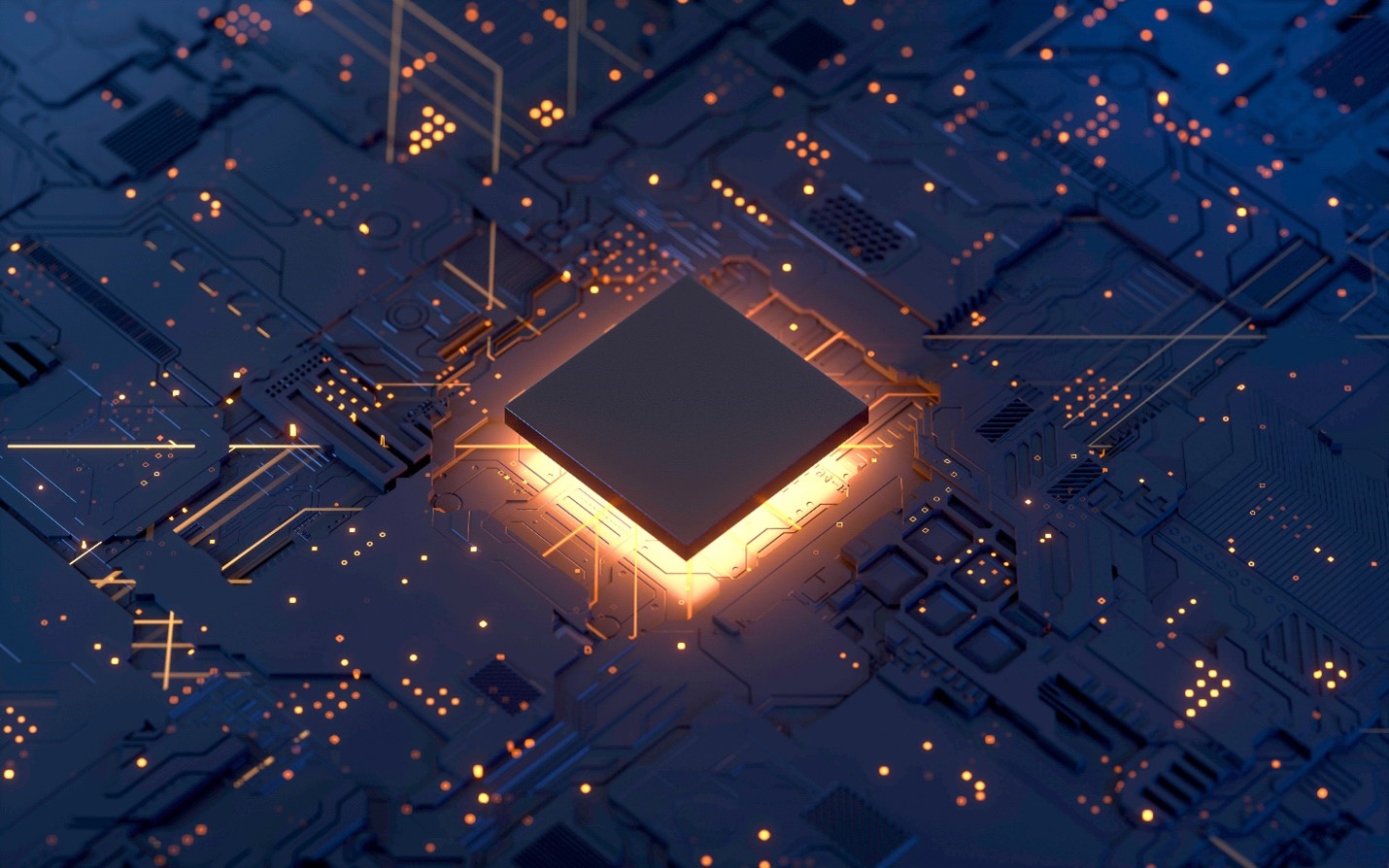
Cutting-edge chips are truly a marvel of engineering.
The individual chips are made from wafers… And a single wafer is made up of hundreds of smaller chips – the little squares on its surface.

A finished wafer from TSMC (Source: Taiwan Semiconductor Manufacturing Co., LTD)
Each wafer is made of dozens of layers. And each layer is etched and then sandwiched together.
Billions of transistors are etched onto each chip… And every single one has to work for the highest-end chips.
It’s these high-end chips that are the hardest to make.
But to make better chips, the transistors need to get smaller.
During the 1990s, cutting-edge chips had transistors that were 350 nanometers (nm).
Advanced chips such as Nvidia’s H100 use 3 nm transistors.
The realm of 3 nm plunges us into dimensions that are harder to grasp. A single strand of hair is 80,000 to 100,000 nanometers wide.
A single silicon atom has a size of about 0.2 nm. So, 3 nm is about the width of 15 silicon atoms lined up, side by side.
As you can imagine, it’s extremely difficult to etch something that small.
But that’s what extreme ultraviolet (EUV) machines are built for…
To start with, the machine blasts particles of molten tin with a laser.

EUV machine firing lasers and droplets of molten tin (Source: CNBC)
This constant stream of tin reacts with the laser and emits EUV rays.
The wavelengths of these rays are so small they’re even absorbed by air. This machine has to operate in a perfect vacuum.
It then uses the world’s flattest mirrors to redirect the EUV light to the wafer.

EUV light being redirected at the wafer using mirrors (Source: CNBC)
The beams of light are held steady, and the wafer is moved to allow the etching to occur.
Each wafer has hundreds of chips. And each chip has billions of transistors.
These machines can make up to 3,000 wafers per day.
Here’s a clip of the entire process…

An EUV machine at work (Source: CNBC)
These EUV machines cost more than $200 million and are the length of a school bus.
The finished product is transported by three 737 airplanes and 20 semi-trucks to their final destination.
And housing these machines is even more expensive. While a basic semiconductor plant making chips for TVs and appliances might cost a few hundred million… a state-of-the-art facility will cost billions and take years to build.
That’s why Altman isn’t wasting any time trying to realize his ambitions for more chip plants.
Last week, Taiwan Semiconductor Manufacturing Company (TSMC) announced its latest earnings.
I won’t bog you down with the nitty-gritty details… The major takeaway is that demand for these advanced 3 nm chips is through the roof. Here’s a statement from TSMC’s CEO, C.C. Wei
We expect revenue from our 3-nanometer technology to more than triple in 2024… and are confident that our 3-nanometer family will be another large and long-lasting node for TSMC.
AI models need to be supported by more powerful semiconductor hardware, which requires the use of the most advanced semiconductor process technologies.
TSMC is the biggest maker of 3 nm chips. It makes Nvidia’s H100 and AMD’s MI300x – the most advanced chips on the market.
But even it won’t be able to keep up with the demand for AI chips.
According to multiple market research companies, AI chip demand is expected to grow by 40% per year to nearly $300 billion by 2030.
Altman realizes that even market leaders like TSMC can’t keep up with demand. That’s why he’s raising money now to build the manufacturing capacity for 2030.
I’ve curated my top picks for semiconductor makers in my Near Future Report advisory. They’re already up an average of 64%… But it’s not too late to get in.
And if you’re not already subscribed, you can go here to check out my presentation on how to profit from AI.
Even if you’re not a paid-up reader, you can still profit by buying the VanEck Semiconductor ETF (SMH).
It holds a basket of semiconductor stocks like TSMC, AMD, and Nvidia. Just remember it also holds companies I think will lag behind, such as Intel.
Regards,
Colin Tedards
Editor, The Bleeding Edge
Like what you’re reading? Send your thoughts to feedback@brownstoneresearch.com.
Read the latest insights from the world of high technology.
There is another type of cage match playing out in Washington right now… The bare-knuckle fight between CFTC Chairman...

The biotechnology sector has shown clear signs of recovery over the past six months…
History suggests that transformative technologies rarely eliminate entire industries. More often, they reshape them. Software is no exception…