



The Largest Merger in History
Tesla and SpaceX have now formed special committees to evaluate a potential merger between these two Elon Musk-led powerhouses.



NVIDIA is showing us where computing is going…
Managing Editor’s Note: Today, we’re handing the reins over to our colleague, Jason Bodner.
Jason’s diving into NVIDIA’s knockout earnings report last week and what it tells us about the direction of AI infrastructure, chips, and computing.
Read on for more from Jason…
NVIDIA delivered yet another spectacular earnings report last week…
Revenue hit $96.2 billion, more than double a year ago. Data center revenue reached $89 billion, up 117%. NVIDIA then told investors to expect another $108 billion this quarter. Even if growth stopped tomorrow, that’s roughly a $400 billion annual revenue run rate.
That’s $12,675.50 per second and higher than the GDP of 80% of the countries on Earth.
But growth isn’t stopping. NVIDIA expects roughly 70% revenue growth next fiscal year, nearly double Wall Street’s expectations. It’s a frankly incredible projection for a company this size.
NVIDIA just gave us a glimpse of the future.
The AI infrastructure buildout isn’t slowing. It’s accelerating. We don’t just need more NVIDIA GPUs. We need more memory, fabs, manufacturing equipment, advanced packaging, power, cooling, networking, and optics.
More. We need a bigger boat.
NVIDIA sells the engines. But somebody has to build everything around them…
NVIDIA’s next-generation AI platform is called Vera Rubin.
Rubin was an astronomer who discovered something strange while studying galaxies. Stars near their outer edges were moving far faster than expected. The galaxies should have been flying apart, but they weren’t.
Something invisible appeared to be providing enormous additional gravitational mass: dark matter.
Rubin’s observations became compelling evidence that the universe contained vastly more matter than we could see. It’s a fitting name for NVIDIA’s next massive AI system.
NVIDIA’s Rubin GPU contains a mind-boggling 336 billion transistors, which raises some fundamental questions…
What’s a transistor? What the heck is a chip anyway?

It’s part of a $4 trillion wave of tech IPOs Harvard calls “the AI IPO Tsunami.” Former IPO insider, Jason Bodner, has uncovered three companies primed to soar as AI companies start going public. Click here to find out how to get their names.

Here’s a “secret” the largest gold miners don't advertise… They're running out of gold. The second-biggest miner on earth is watching its production collapse from 2 million ounces a quarter down to 719,000 – and another major just paid $15 billion for a rival in the biggest gold deal in history, only to see its output stay flat. They can't drill their way out fast enough, so they have to buy their way out. Which means gold just entered its acquisition phase – where the best small miners get bought out at whatever premium it takes. Already, Founder and CEO of Golden Portfolio Garrett Goggin's readers have enjoyed overnight buyout premiums of 40%... 67%... 79%... and the acquisition phase has barely begun. Go here to see details on Garrett's current top three buyout picks.
At its core, computing is remarkably simple: 0 or 1. On or off.
Computers manipulate unimaginable combinations of these two states to calculate, store information, run software, and now, to generate artificial intelligence.
Originally, those switches were vacuum tubes. ENIAC, one of the first general-purpose electronic computers, contained roughly 18,000 vacuum tubes, weighed about 30 tons, and filled a room.
If more computing required more switches, we couldn’t keep building bigger rooms.
So in 1947, Bell Labs invented the transistor – a tiny electronic switch with no moving parts that could eventually become microscopic.
The next breakthrough was putting huge numbers of them together on silicon.
Why silicon? Materials have three basic electrical behaviors:
Silicon is a semiconductor, making it perfect for microscopic switches. Eventually, we learned to manufacture both the transistors and their connecting circuitry directly onto silicon.
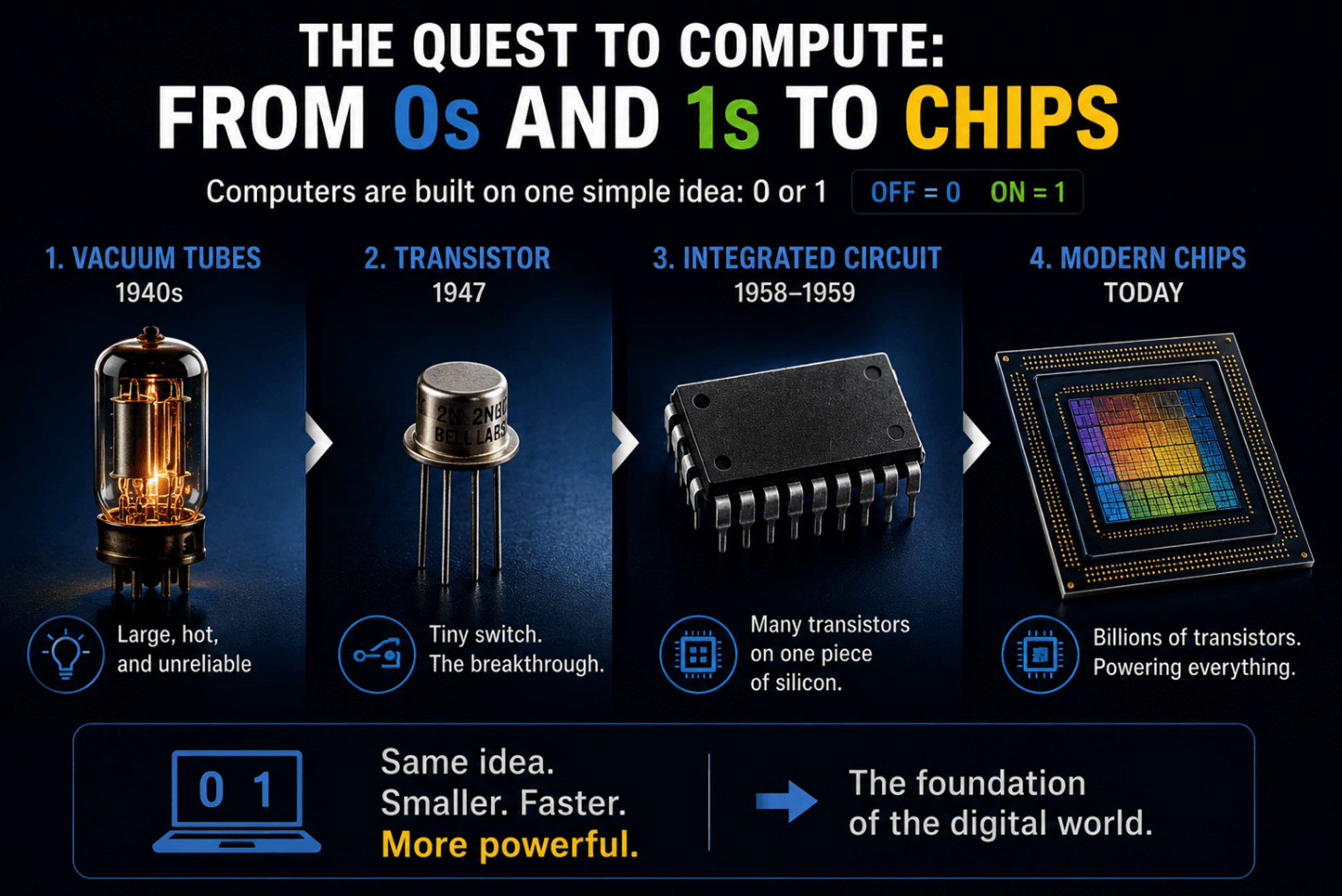
The integrated circuit was born.
For nearly 70 years, we’ve been shrinking it. Today, NVIDIA can fit 336 billion transistors onto Rubin.
So how do you build something that small?
You start with incredibly pure silicon, sliced into thin discs called wafers.
Then the machines take over.
Think of semiconductor manufacturing almost like microscopic 3D printing combined with photography and sculpting. Machines deposit incredibly thin layers of different materials. Light patterns the circuits. Other machines etch material away.
Deposit. Pattern. Etch. Clean. Measure. Inspect.
Repeat the process hundreds of times until a blank wafer becomes a three-dimensional structure containing billions of transistors and microscopic connections.
Think about that: human beings invented machines capable of manufacturing structures we can’t even see.
Collectively, these machines are called Wafer Fab Equipment, or WFE.
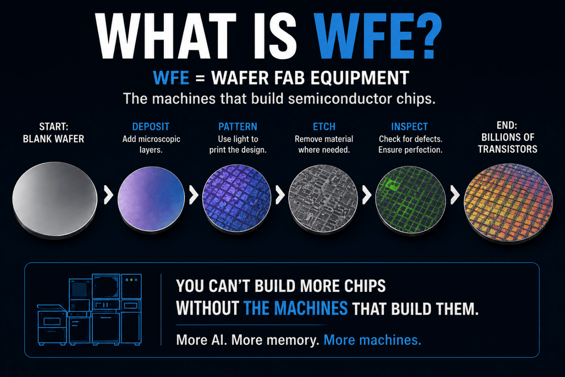
And if AI needs dramatically more chips, the world needs dramatically more equipment to manufacture them.
SEMI projects worldwide 300mm fab equipment spending will reach $133 billion in 2026 and $151 billion in 2027. Memory equipment investment alone is projected at $52 billion this year and $57 billion next year.
But manufacturing individual chips isn’t enough anymore.
For decades, more computing power meant making transistors smaller and putting more of them on a chip.
We’re still doing that, but physics makes shrinking increasingly difficult and expensive. So the industry found another path… connecting sophisticated chips.
A modern AI accelerator combines a massive GPU with stacks of HBM, or High Bandwidth Memory. The GPU can perform astonishing amounts of computation, but it’s useless if you can’t feed it data fast enough. HBM puts extremely fast memory right beside it.
Now all those pieces need to communicate at extraordinary speeds.
Enter: advanced packaging.
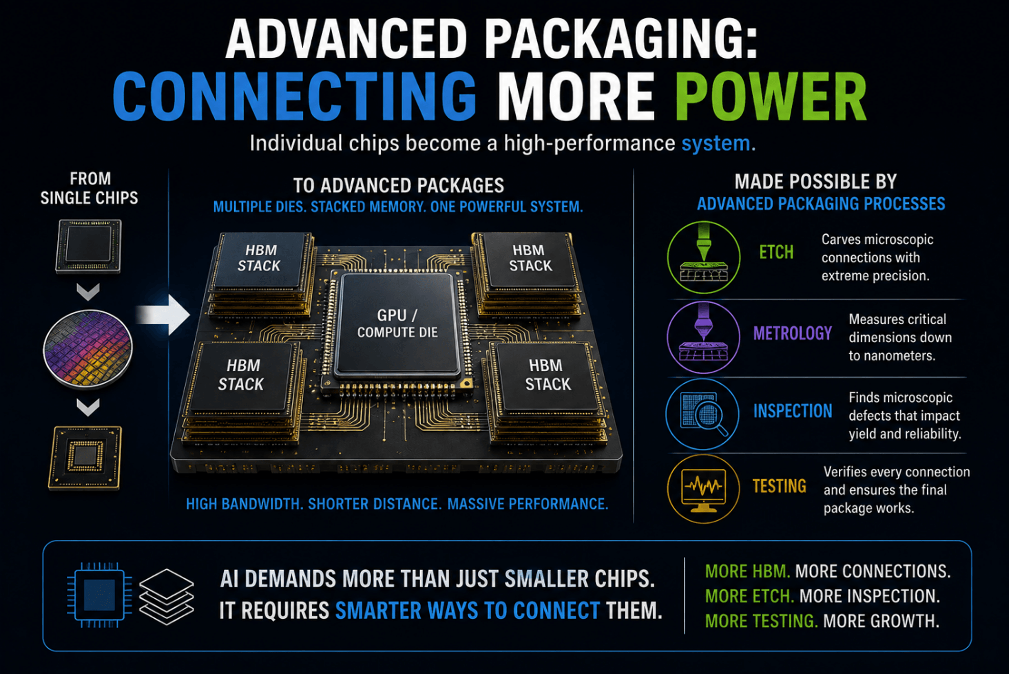
We’re building integrated computing systems from multiple pieces of advanced silicon. That requires increasingly sophisticated deposition, etching, metrology, inspection, and testing.
More complexity means more opportunity.
Then you have to move the data… and here comes another bottleneck.
Copper is fantastic at moving electrical signals over short distances. But AI requires enormous amounts of data to move between chips, servers, racks and data centers.
As bandwidth and distance increase, electrical connections face problems with power, heat and signal loss. So increasingly, we move from electrons to photons through optical networking, silicon photonics and eventually co-packaged optics.
Vera Rubin already includes networking designed to support both traditional pluggable optics and co-packaged optics.
Now look at the whole picture…
WFE builds the chips. HBM feeds the chips. Advanced packaging connects the chips. Photonics moves the data.
Then add the power, cooling, networking, and data centers required to run everything.
This is why investors make a mistake when they look at NVIDIA’s results and see only NVIDIA. You cannot deliver this kind of growth without enormous investment taking place underneath it.
AI is a stack of technologies where solving one bottleneck leads to the next. More compute requires more memory. More memory requires more manufacturing. More manufacturing requires more equipment. More sophisticated systems require advanced packaging. More data requires networking and optics.
And all of it requires more power.
Nearly 80 years after Bell Labs invented the transistor, we’re still building on the same fundamental idea: on or off, one or zero.
Except we’ve gone from 18,000 vacuum tubes filling a small house to hundreds of billions of microscopic switches inside a processor that fits in your palm.
That’s about 19 million times more switches.
NVIDIA is showing us where computing is going…
The opportunity is everything the world has to build to get there.
Regards,
Jason Bodner
Founder, Outlier Intel
Add Brownstone Research as your preferred source on Google to see our latest stories in your feed.
 Add as a preferred source
Read the latest insights from the world of high technology.
Tesla and SpaceX have now formed special committees to evaluate a potential merger between these two Elon Musk-led powerhouses.

This isn't about simply recreating the old system on new infrastructure…

As companies give digital workers more responsibility, protecting their systems becomes part of the cost of putting AI to...