

Will OpenAI Go Bankrupt?
In today’s AMA, we explore the true utility of full self-driving vehicles… what to do when markets crash… and...



Musk isn’t planning on following the same playbook as the rest of the semiconductor industry.
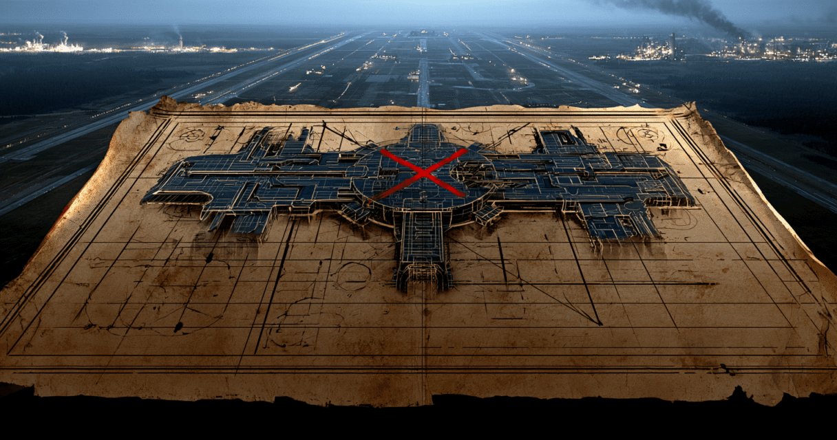
Last week, we got a look at Elon Musk’s vision for the Terafab.
It’s a combined effort between SpaceXAI (SPCX) and Tesla (TSLA), and the goal is to build the world’s largest semiconductor manufacturing plant.
The Terafab will produce advanced semiconductors, memory, and advanced semiconductor packaging all within a 100 million square foot building.
The scale is almost impossible to understand.
Below is a rendering of what the actual Terafab will look like once completed. It’s stunning.
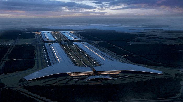
Terafab Rendering | Source: SpaceXAI
It is a breathtaking vision of an optimistic future.
It looks like it came out of a science fiction movie.
Musk says, “Terafab Texas will be the largest and most valuable building on Earth by far.”
As always, the media clowns have piled on again.
This one from Fast Company with the headline, “Terafab could become the largest factory on the planet – or Elon Musk’s biggest failure,” which went to lengths to sow doubt and even referred to the project as “fantasy.”
The ignorance is stunning and completely ignores reality.
This April, Tesla already broke ground on the north campus of its Gigafactory in Austin, Texas, for its Terafab prototype manufacturing site.
The first production semiconductors will be manufactured late this year, entering full production in 2027.
This location will enable Musk and his team to iterate quickly on semiconductor manufacturing processes in preparation for the construction of the Terafab in Grimes County, the groundbreaking of which is imminent.
The initial phase of the Terafab project is $16.8 billion, with the total capital investment to complete the 100 million square feet Terafab at $119 billion.
What’s the motivation for Musk to take on such an ambitious project?
It’s simple.
Musk needs these advanced semiconductors to:
And that’s not to mention the normal production of Tesla’s Model 3 and Model Y self-driving electric vehicles.
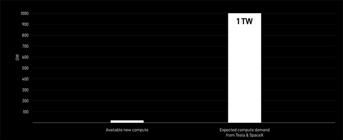
Tesla/SpaceXAI Semiconductor Needs vs. Industry Capacity
Source: SpaceXAI
What the semiconductor industry can currently supply is a small fraction of what Tesla and SpaceXAI need for future production.
Terafab will close the gap.
Musk and his companies will take as much capacity as they can get from TSMC (TSM), Samsung Electronics, and maybe some from Intel (INTC) in the future.
But he has no choice but to build out dedicated manufacturing capacity.
The vertical integration built into Tesla and SpaceX is a core competitive advantage for these two companies, both of which have transformed their respective industries.
And to put the costs into perspective, SpaceXAI has $100 billion in cash from its recent IPO, and Tesla has $43 billion in cash.
Musk has the money to execute on his plans, and if there is one thing I’m sure of, he can raise additional capital if he needs to in order to complete the project.
The reality is that no other executive in history has the track record of successfully executing on bold, ambitious engineering projects like Musk.
And whether it is enabling patients to control computers with their mind (Neuralink), tunneling under the ground (Boring Company), dropping launch costs to orbit by 99% (SpaceX), developing artificial general intelligence (xAI), or inventing self-driving cars and intelligent general-purpose humanoid robots (Tesla), Musk has always invented novel engineering approaches that industry has never seen before.
Which leads us back to the Terafab.
Most believed that Musk would just do the same thing that the rest of the semiconductor industry is doing to produce advanced semiconductors, which is using ASML’s (ASML) EUV lithography machines.
But the images revealed last week by Tesla concerning the Terafab revealed something far more interesting – only visible to a trained eye.
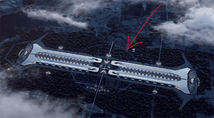
Take a look at the Terafab facility, but this time from an aerial view:
Source: Tesla
Notice anything unique?
Centered in the middle of the Terafab is a thin-lined circle that provides further symmetry to the architecture.
To most, that looks more like something for aesthetics.
But to those familiar with bleeding-edge semiconductor manufacturing, it means something entirely different.
That circle represents a future particle accelerator, which is designed to accelerate charged particles to extremely high speeds by using magnetic fields.
The particle accelerator can be used to create high-intensity light beams, far more powerful than ASML’s EUV technology, for use in semiconductor manufacturing.
This approach is referred to as Free Electron Laser (FEL), as opposed to ASML’s approach to EUV.
ASML’s process involves vaporizing molten tin droplets in a vacuum with high-powered lasers. This creates a superheated plasma that gives off EUV radiation used for semiconductor production.
FEL avoids this process entirely by using a particle accelerator to produce 4 times the amount of EUV power. The advantage of using FEL for semiconductor production is that you can reduce EUV cost by 50% and lower total wafer cost by around 20%.
Oh, and you can potentially double semiconductor production at even higher yields.
While all of this may appear to be speculation, Musk was kind enough to confirm on August 6 that the tech community in the know was right…
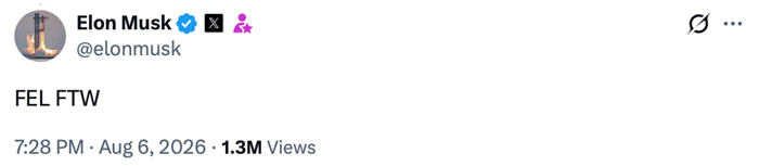
Free electron laser… for the win!
Musk isn’t planning on following the same playbook as the rest of the semiconductor industry.
His goal is to leapfrog it.
There are a few companies I know of that have been working on FEL technology to produce semiconductors. One is xLight.
And the executive chairman of xLight is Pat Gelsinger, the former CEO of Intel.
In addition to xLight, there is also Inversion Semiconductor, and also Austin, Texas-based Tau Systems.
I have no idea whether Musk is making a deal with any of these companies for collaboration on FEL technology…
But if I had to guess, he’s going to acquire one of these three companies to bring the talent in-house and make this radical new approach to semiconductor manufacturing a reality at the Terafab.
And by doing so, he will achieve something never done before in the semiconductor industry, just like he has done with every other technology he has worked with.
The Terafab is real, it has funding, and it is most certainly not a fantasy.
It’s just an engineering challenge.
And in the next few years, it will indeed become the most valuable building on the planet, and more important than that…
… It will accelerate our path to an abundant future.
Add Brownstone Research as your preferred source on Google to see our latest stories in your feed.
 Add as a preferred source
Read the latest insights from the world of high technology.
In today’s AMA, we explore the true utility of full self-driving vehicles… what to do when markets crash… and...
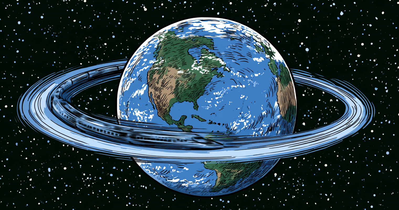
Only one form of transportation has felt futuristic for decades… like a mirage always on the horizon. Never close,...
We’ve been waiting for future forms of commercial transportation for decades, and finally that time has come.